Category Archives: Mark-8 Clone Project

… Or maybe it’s not that easy

Okay so let’s start with what I had to do to make some period correct looking Mark-8 PCBs.

One thing I’ve had to learn the hard way with the toner transfer PCB-making process, is that it really relies on good quality artwork.  If you’re working third-hand with someone’s low quality scan of original artwork, you’re going to have a problem.

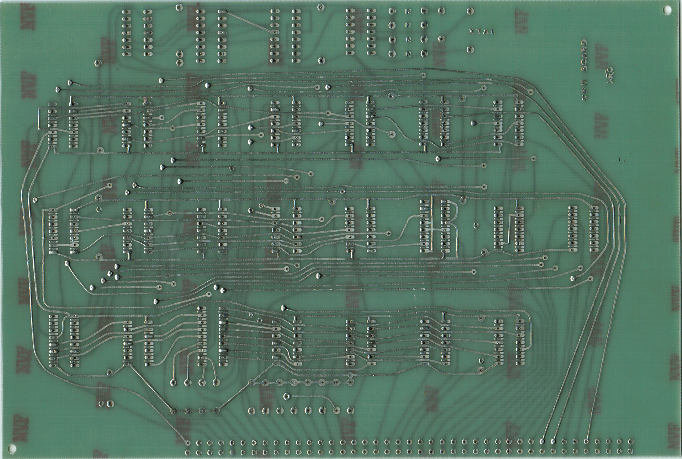
While initially my first attempts at making a double sided Mark-8 CPU board looked successful, when I examined the finished product more closely with the eyes of experience from my TVT project, I realized it wasn’t.  Looking closely at the traces, I could see a ‘pixelated’ pattern which I think was a result of the dithering from the low resolution, greyscale scan I had been working with.

Some months after I made that first board, I came across an auction for an original TV Typewriter.  I lost, but the seller, a generous fellow named Roy, offered to send me a ‘consolation prize’ in the form of an original Mark-8 construction guide!  Having an original booklet in my hands meant I could experiment and try to get the best possible scan quality, with an eye towards making new boards rather than just archiving history for others to read.  I would try to get the traces as dark and thick as possible, to better accomodate my  “ironclad” toner transfer procress.

The first thing I did (carefully) was fool around with my guide and my day-to-day Brother all in one scanner.  However, the scanner’s top end resolution is only about 600dpi, and I was finding it was distorting the artwork dimensionally.

I then remembered that I had a much, much better scanner tucked away in a closet.   This was a professional photo scanner, given to me by a late client of mine.  It is a Microtek i900, an older scanner but with a still-impressive 6400×3200 resolution capability.  The resolution in particular is fantastic – I’ve actually been able to scan stills from 8mm film and get pictures out of them!

Microtek gives you a pretty nice interface software-wise.  I am setting this to a strict black and white line art mode.  Getting the traces perfectly black is very important.  Greyscale printing at less than 100% black means you run the risk of having thin traces.  I want my Laserjet 4250 to paint those traces on nice and thick.  I also want to have pure black and white (line art mode, to the scanner) so that there is no in between anywhere I don’t want toner – no ‘grey’ patches that will resist my etchant, leaving me with unsightly splotches or bridged traces.

To really make sure I get it all, I set the scanner to 1200dpi.  It takes a couple of  minutes at that resolution to get it all in, but the result is fantastic – crisp and clear with no fuzziness:

I decided to print it off on an overhead transparency sheet to compare it to the original.  To my amazement, there is no distortion whatsoever.  The scanner rendered a perfect copy!  Yahoo!

Now I need to clean these up and prep them for transfer to copper.  One thing I will take the opportunity to do here is put some pin holes in the IC pads.  This will make drilling easier.  I’m doing this all one one side, and only in a few places on the other.  It’d be difficult to get all the holes lined up properly so I’m sort of saving some energy here.  I’ll simply drill from the side with all the hokes, and then use the few I’ve made on the other side for aligning both boards.  I’ll also flip them so that they come out the right way when ironed on.

Just as I did with my first attempt, I need to use Photoshop to get the two sides nicely aligned with one another so that when they are produced as a board, there won’t be any pads or holes out of place.  I made a good call in checking this, rather than trusting that if my transparencies matched the plans, all would be ok.  As it turns out, the two sides for each board in the plans do not always align!  I don’t know if this is printing errors, or the effects of 45 years of humidity changes, but they definitely do not.  So here’s photoshop at work again.  Basically what I do is temporarily convert the images to grayscale (this allows me to create layers).  I then copy one side of the board I’m working on and paste it over top of the other.  I then scale back the opacity on the new ‘layer’, such that I can see through it somewhat.  This’ll let me get them lined up.  For the actual line up process, I’m using a variety of Photoshop tools including scale and warp.

With that squared away, I move on to toner transferring and etching.  First I print them off on my Laserjet 4250 on the ‘super glossy’ setting, which prints nicely on magazine paper (and slowly).  As I’ve mentioned before, I use my totally unpatented 2-5-2-2 process to get a nice crisp image from my iron.  It really helps that my printer lays on the traces nice and thick solid black here.  What a help that is.

When I’ve got both sides for a board ready, I trim them with my scoring tool, and then dip them in my vinegar/salt/peroxide bath.  I’m still feeling my way around with this process but I’m learning that it’s better not  to apply the salt directly on the copper.  It actually can cause pitting and even will peel the toner resist away from the board, which wrecks your traces.   Another thing that can happen: put too much salt in and it will cause a very strong reaction with can discolour the PCB substrate with an ugly yellow/green.   To avoid all that, I pour the salt in alongside the board and then just sort of swish the etchant tub back and forth gently.  I set the whole thing in a sink of hot water to help the reaction along.  Anyway, it’s a slow process but it seems to leave the PCB unscathed.

Now here’s the hard part – gluing the two sides together.  I thought this would be easy – just paint some epoxy on both sides, press em together and…

Meh.  I mean, it’s functional — the epoxy works, but I’m left with these ugly splotches, like the one on the lower right in the photo.  What I find out the hard way is, the epoxy is almost impossible to brush to a consistent level across both boards.  This produces spots of varying sizes and darkness when you press them together, which do not look period correct or correct at all.  I’m trying to make these boards look like they were original single piece double sided boards.  That is not what we are getting here.

I’ve got to think about this now and try to figure out how to make this work.  Some have suggested getting a book press to clamp the boards tightly and squeeze all the air out.  But that’s another expense for something I won’t use that often, and book presses are pricey as well as heavy!  Hmm.   I think before I go that route, I’m going to have a look at other adhesives…

Mark-8 board do-over

As I mentioned in a previous blog post, I got lucky and came across a whole bunch of vintage, produced-in-1973 Synthane Taylor boards.  The production date codes were 1973, as verified by the still unopened bags they were in:

Pretty amazing that these had sat unused all these years.  And as mentioned, they bear the same little ‘Tc’ marks on the PCB substrate that the originals do (albeit different colour):

Previously I had posted that I thought these were the marks of Techniques, the company that produced the original kit boards back in 1974.  I have since determined that Tc actually stands for Taylorclad.  Techniques, I believe, did not make the substrate or blank copper clad stock that was ultimately used for the kit boards – they were just contracted to lay them out, etch, tin and package them for buyers.

In other blog posts I’ve mentioned my disappointment, as someone who desires a replica that is as close to original as possible, with modern PCB stock.  It just doesn’t look right, which is obvious in photos.  Again, compare an original Mark-8 board (right) to one I produced on modern copper clad stock (left):

It might not be immediately obvious to the untrained eye, but it’s definitely something I notice.  So I’m grateful these boards have been available.  The fact that they are only 0.030″ thick vs. the standard thickness of 0.060″ actually works to my advantage; I can simply make one side of the two sides, then the other, on two separate sheets, and then bond them together….

Preparing and etching the Mark-8 CPU clone board

Okay so on my last post I had tweaked artwork and set up for trying to make a copy of my Mark-8 CPU board.  I got my double-sided copper clad in yesterday and am raring to go!

In terms of process, it’s very similar to what I went through with my TVT boards.  The difference this time is I have an original for reference and can be a bit more confident that my work is good.

The first thing was to print out the artwork on my favourite Hot Rod Magazine paper.  I don’t know why but this stuff transfers really well.

The challenge with doing a double-sided board is getting both sides to align just-so so that your ICs and components will install easily.  This is why I went to some lengths to make sure the artwork matched properly in Photoshop.  Now I had to align it on the copper clad.

The strategy I settled on was to drill holes in a couple of IC and resistor pads up top and below.  I reasoned that these were so small that if they aligned okay, I knew I’d be good.  I then made holes in the appropriate places on the artwork.  I used a small piece of wire to go through the PCB and transfer paper and bent on one side to secure.  I did this in three locations just to be safe.  In the first photo you can see the little pin through on the other side.

Basically from there it was just carefully aligning the transfer sheet for side two to those pins, and once the pins were through bending them to hold it in place.  Then I took some scotch tape and pressed it down on the corners to hold.  I didn’t want the pins staying in and damaging the iron or ripping the paper, obviously as I ironed.

Ironing went fairly smoothly, however I did note that the resulting heat caused the opposite side I was ironing to actually smudge the toner in a couple of places.  Hrmm.  Not sure how to get around that.  Perhaps having the ironing happening on something cool?  The counter top does get pretty hot when I’m doing this.

When I dipped the boards into the cooling bath and removed the paper, I discovered, as usual, the iron had missed in a few places.  Almost always does.  So I did touching up with nail polish to fill gaps.

Anyway, once that was done, I used my original board (very carefully) as a guide to trace cutting lines so I could cut the board to be the exact same size.  Voila, side by side:

Next was etching.  I’m still wussing out from using heavier stuff like my ferric chloride.  I think I might be getting over that.  One problem with using the friendlier vinegar/peroxide/salt etchant is that it takes a ton of it to etch boards this big.   I used 6 500ml bottles of peroxide and an equivalent amount of household cleaning vinegar.  It took something like 2 hours to etch off the acres of copper on this board that needed to go.  And unfortunately that’s too long for the nail polish ‘patches’ to hang on.  The nail polish eventually lets go and that copper becomes exposed.  I had to apply it again to try and save those traces, but a few were eaten right though.

Overall the result after etching isn’t too bad.  Side 2 came out really nice and clean.  I think I have to do more work on Side 1’s artwork to make the traces a bit darker and a tiny bit thicker.

Lastly I took some acetone and wiped away the toner.  Then I drilled out some of the pads to test how both sides aligned.  I’m delighted to say the alignment is just a hair off in a few places.  But otherwise, it’s darn near perfect, especially considering the bozo (me) trying to align them.

So there you have it.  I’m going to use this board as an experiment piece.  I want to see if dying it with some blue or green Rit dye gets me a bit closer to the color of the original (right).  Then I’ll learn about tinning, and just see how close I can dial it in.

To recap: I need to figure out how to better transfer toner.  I’ve stuck with ironing because it has served me well.  My laminator did not do a good job and these fancy transfer papers seem to be even less reliable than my magazine paper.  I also need to maybe adopt a better etching process.  But for a first try, I’m pretty happy.  This gives me confidence that the end goal is attainable.

Mark-8 Clone Project Begins

Christmas is done (yay!) and now I have a bit of free time before we go back to work for vintage computer projects.  And what better way to close out the old year and ring in a new one by attempting to clone Jon Titus’ Mark-8 boards?

In earlier posts I detailed my adventures in recreating the board set for Don Lancaster’s TV Typewriter.  That project is still ongoing, but by far the most fun I had was taking scans of the original artwork and then transferring that onto copper, and I’ve been looking for excuses to make new PCBs for something else.

Recently I acquired some original, untouched Mark-8 boards on Ebay.  That remains the pinnacle of my collecting career, given how rare these are.  However I bought them without really thinking through what it meant.  Boards alone do not a computer make, and to take a soldering iron to these means risking damage, both literal and in terms of value.  There are only around 20 or so Mark-8s known to exist, and of those, only mine and one other set are known to be unbuilt.

I’m not totally against building them though.  I solicited opinions all over the place and many were of the mindset that a computer is pointless if it doesn’t do anything.

It’s a tough one.  But in the interim, there’s no crime against history in recreating some new boards.  At the very least, I can use them as practice runs for potentially building these ones one day.  Better to learn on something that isn’t virtually irreplaceable first.  I’m therefore setting a goal of recreating new boards that look as close to the originals as possible.  I’ve even read up on how to dye my new PCB stock to more closely match the color of the original, and even how to create a stamp to mark the boards with the similar marks the PCB fab house would have used.

To be clear, cloning the Mark-8 boards has been possible all the way back to day one.  The original construction guide provided the artwork to make your own.  In fact,  Steve Gabaly (aka Obtronix) took copies of said artwork and produced a kit, which some unethical types occasionally tried to pass off as original on Ebay.  I’m told these kits had some issues, owing to the quality of the copied artwork they were based on.

I had actually planned to go the same route myself using a PDF of the construction kit Bryan the ‘Byte Collector’ was kind enough to scan and put on his site.  That had been my original ‘get a Mark-8’ plan going back years.  I “knew” the odds of affording, let alone seeing a Mark-8 for sale anywhere were slim to none.

I was warned though not to trust the construction guide copies found online.  Copying and scanning does funny things to artwork.  I ran into this on my TVT build:  the artwork had to be scaled up slightly to fit components properly.  Lacking an original TVT to compare to, I’m still not sure I’m 100% in the zone, but checking against ICs and components, they look right.

An additional challenge: Mark-8 boards, unlike the TVT, are double-sided.  I’ve never made double-sided boards before.  I’m lucky the originals weren’t (for cost reasons) through plate – I’d never be able to do that myself, so at least mine can still be in keeping with the originals that way.  But I know lining up two distinct pieces of artwork and making it come together just so will be a huge challenge for someone of my limited skills.

However, I do have the advantage of having the original boards to compare against.  Further, a Mark-8 clone would be the perfect companion to my TVT clone – both were signature Radio Electronics magazine projects, and in fact the Mark-8 information mentioned the TVT as a possible interface device.

Now, originally I was just going to import the scanned artwork into Photoshop and then keep tweaking the size and printing it until the IC pads fit the ICs, which I have.  But since I have the originals, I have an advantage others didn’t.  So what I’ll do is actually scan the originals on my scanner.  That’ll give me something visual onscreen to compare to.

The first thing I did was put it (gently) on my scanner.  I didn’t need anything high-res here, just good enough to clearly see the traces.  The result (of the first side):

A direct scan of my original Mark-8 CPU board.

Pretty elegant, huh?

After converting the artwork in the PDF to JPG, I then imported the first side of the CPU board artwork into Photoshop.  Next, I opened up the scan I made of the original in a separate window.  I realized I had to do a bit of scaling to get the artwork into roughly the same size as the original. So I went back to the artwork, rescaled it, and then used the marquee tool to highlight and copy all of it.  Now I brought it over into the other window and pasted it as a second layer.  This of course completely obscures the original board below, however by changing the opacity of the new layer (called Layer 2) over on the right side of the screen, I can make it so that I can see through the artwork I’ve pasted to the original below.  This will help me align the two and do any changes necessary to make them as close as possible.

Okay so obviously I needed to further reduce the size of the artwork, which I did.  However, reducing wasn’t enough.  Looking at the two interspersed with each other it became really apparent just how skewed the scanned artwork was.  It wasn’t, like the TVT, just a matter of being the wrong size.  It was actually distorted in a sort of trapezoidal shape.  Thank goodness I had the originals to rely on.  If I’d tried to make a go of it with these, I’dve been hopelessly lost!

Anyway, since I have the original to use as a guide, I’d just have to make use of the appropriately named Distortion tool, and Skew tool, to fix the messed up artwork.   After half an hour of carpal tunnel-inducing fine mousework, I had them more or less aligned.  The screenshot below shows me about 90% of the way there:

After getting it the rest of the way, returned the opacity to 100%, did the marquee tool and copied the now-corrected artwork back over to the original window.  After clearing that window and pasting it there, I then flipped it horizontally (since I intend to use the toner transfer method again this is necessary to prevent it from producing a mirror image when applied to the copper clad board), whitened up the background and saved it.  Then I printed it off and using a bright light behind compared it to the original board.  It aligned almost perfectly!

Having completed that side, I turned my attention to the other side of the CPU board.  I followed the same process, scanning the backside of the original, importing the artwork and so on.  The back side was even worse than the front.  It was way off, and I really had to work that distortion tool to get it correct against the original.

After completing and saving it, I decided to check not only how it compared to the original but how it lined up with the first side artwork I had fixed.   To my surprise, it didn’t quite line up right.  In fact, some of the bus holes were as much as several mm off!

Hmmm.. how to fix that.  Aha!  I’ll use the two sides of the corrected artwork and align them against each other.  I figured the easiest way to achieve this was to invert one side (making the black and white colors reverse), and then copy the other side over it, and set opacity down to 50% on the copied layer.

Then it was just a matter of making the black traces of the copied layer line up with the white ‘spaces’ of the inverted layer.

It took a bit more finagling, some rotation and so forth before I had it pretty much dead on.  Once that was done, I again brought the opacity of my Side 1 layer back to 100% and then copied over to a new, clean window.  I reversed the inversion on Side 2 and saved both.

Now I have nice , fairly correct artwork for the first board:

Yes, I did make one tiny alteration.  The construction article artwork doesn’t have the manufacturer’s (Techniques) mark right beside where it says ‘CPU BOARD’.  I actually copied that from my originals, converted to black and white and touched it up and then pasted it to my artwork.

The print copies of the artwork line up nicely when put together:

And they look pretty good dimensionally next to the original board:

The artwork is nice and dark and should transfer pretty nicely.  I can’t wait for my double-sided PCB stock to arrive so I can try it out!