Progress continues on my TV Typewriter Redux project. After encountering disaster in the form of weak traces, I cleaned up and readied my second TVT mainframe board (there were three, thankfully I got one right!). It looks great – the dye isn’t quite as blue as on the last one and it looks about as vintage as I think one can make modern PCB stock look.
I don’t yet have the transformer, fuse clips, or self test posts. I’m also missing two momentary return DPDT switches. But I’ve installed pretty much everything else. The mainframe is easy to work on – everything is spaced out nicely.
Moving up the unit I started work on the Cursor board. I had run out of old 14 pin sockets from my parts bin, so I hunted ebay and found these blue Cambion wire wrap sockets. I don’t know what year they’re from but to me they look a lot like the ones my new friend Roy used on his TVT:
You can see Roy installed them only for certain ICs. I suspect this was a decision based on what was likely to fail, and what components were too expensive to risk when doing self-tests and/or diagnostics. But where he used sockets, they are those nice, tall blue ones. I don’t know if they’re wirewrap — doubt it — but I can just install my wirewraps and trim the legs and get the same look. Here they are installed with ICs in place.
I didn’t exist yet in 1973 but I think that looks pretty authentic if I do say so myself!
You’ll note I also did a test fitment, plugging the Cursor into the Timing board and then the Mainframe underneath. It had occurred to me that if the Mainframe scan was skewed there was every likelihood the others were as well. But I had hoped because I made sure to compare the three smaller boards before etching them that they would work.
I can’t say they fit perfectly, but they can be made to fit, and continuity is perfect between boards. I can easily trace connections from a pin up top to where it ends up on the mainframe. Excellent! One small beef – although the first board plugs nicely and snug into the mainboard, the others sit up about a quarter inch from the molex connectors beneath. I figured out this was because I had soldered the pins in such a way that they were actually pressing against the bottom of the molex connectors, restricting how far the pins from above could penetrate. I’m not sure if I’ll attempt to remedy this at all, or just trim the pins on each board to compensate. Hmm…
One of the unantipicated tricky parts of trying to make my prototype look authentically oldschool is finding components that look correct for the period. As we know, as technology advances things tend to get smaller, and indeed, capacitors in particular are much, much smaller for the same capacitance than they were 40+ years ago.
One cap that has really annoyed me from the beginning is the 100uf. These are used all over the place in the TVT. If you recall my ASCII encoder side project, you’ll recall just how tiny those 100uf caps were relative to the originals. Here’s a pic of one for a refresher. They are absolutely puny:
I realize my artist’s OCD is at play here, but still. I want this thing to look right. These do not look right. I mean, the ‘metal sausage’ look could be authentic. Shortly after Christmas, an auction for an original TVT appeared (sadly, I lost it, but more on that in a future post). The owner/builder, Roy, was kind enough to send me some photos of it. It’s amazing to have some quality photos of an original. This shot of the memory board shows that indeed, metal sausage caps were around back in the day:
But again, they are quite a bit larger, and they are not what Don used in the prototype. For perspective, here is what the originals should look like:
They’re basically a mini can. They have a very nice, flat top, cylindrical look. The cap pictured is a vintage Siemens 100uf 16V. These are all over my SWTPC equipment and appear to be similar to what Don used on the TVT.
I hunted and hunted for months. Finally, I had some luck. Somebody had these lovely ruby red Bakelite-style caps that were the exact same size and style as the Siemens I was looking for!
I couldn’t find any in any color other than red, but that was fine with me. I’ve accepted from the outset that I was never going to get an exact copy of Don’s prototype internally. There’s just too many unknowns and long discontinued parts. But these will do! I’ve ordered a whole bunch and will install them wherever 100uf are required, and also use them to replace the ones on my ASCII encoder to remove that bit of modernity. Hopefully they work!
So I’ve got my TV Typewriter ‘mainframe’ parts install underway. I’ve got molex connectors, caps, diodes, resistors — the whole nine yards. I decide to put the board up against a light to check for any trace ‘bleeding’ or accidental solder bridges and then:
Not good. Not good at all!
This is something any homebrew PCB maker should check before proceeding. I had been fooled — from topside, the copper obscures the tiny pinholes visible here. Since these pinholes look like the pattern of pixels in a magazine photograph, I’m guessing not enough toner was deposited to fully protect them from the etchant.
Interestingly, the traces all test good on the ohmmeter. I’m tempted to carry on – but this state of affairs really bothers me. More experienced hands warn it will eventually fail. So I decide to switch to the second mainframe board I made — that one passes the backlight test handily. I’ll wipe the black silksreening off it, clean it up, check it, and transfer everything over. Thankfully the mainframe doesn’t have too many parts installed!
Just for clarity, what Radio Electronics refers to as ‘the Mainframe’ is what you and I today would call the ‘motherboard’. Just to clear that up in case it causes confusion among those who think of mainframes as something else entirely.
I ended up making three motherboards. The first was my first-ever homemade PCB; and it showed. I rejected it outright for overetching and bad cutting. The second was much better, but had a few spots of copper remaining where I didn’t want it. I decided to use that one to try doing ‘silkscreening’ on the backside using laser toner. The third board is the one I’m starting with. It benefitted greatly from my newly acquired knowledge about etching, cutting and so on, and looks really clean. Let’s get started.
I should note I decided late in the game to forgo silkscreening altogether on my prototype. I don’t know why I was so fixated on it. As we can deduce from this photograph, the prototype does not have it:
So that lets me off the hook. And anyway, the original silkscreening on the SWTPC kit boards was white, and since I don’t have a (expensive) printer that can print with white toner and I’m not willing to shell out to make an actual silkscreen, I’m going to leave the silkscreen off.
Again before embarking, I decided to check the appendix at the end of the construction guide for any last minute warnings about the mainframe. Sure enough, there was one. Diode D6 is shown backwards on the parts overlay! Luckily, the overlay I borrowed from SWTPC.com had it corrected already:
I’m glad they caught that 40 years ago and that I didn’t have to spend a week or two puzzling over schematics.
Oh and did I mention the schematics themselves have errors? Yikes! Several corrections are made in the construction guide appendix.
Per the guide, I want to get molex connectors installed first and check fitment. It takes minimal time to drill these out on the PCB and then solder them in:
The Dremel does a decent job, although it does have a tendency to wander. Once you get used to this though it’s easy enough to adjust your entry point to get your holes where you want them.
In the event, I decided to drill out the entire board, carefully looking at the photos from that ebay auction I missed to make sure I drilled the right size holes (more or less). I then couldn’t resist installing some of the capacitors:
Originally I was going to use these vintage looking blue Rubycons for the twin 1000uf caps, but along the way to getting here I found these mint condition Temple units. They look much closer to the prototype’s design and are shorter than the Rubycons, so they fit better on the board. In the end I decided to stack them just as Don did on the prototype. There’s a practical reason for this – the 5000uf cap is huge and cuts uncomfortably into the space you need for the first 1000uf cap. Stacking them frees up room.
I also switched from a modern 4700uf cap to a Mallory 5000uf unit. These tall metal caps are way more authentic looking to the early 70s than the modern ‘sausage’ ones. Unfortunately these caps are the ‘slot terminal’ type. They have three contacts around the outside (for negative) and a fourth on the inside (for positive). I had to jury rig it with 14 gauge wire to make it work with my board.
This prompted some tut-tutting online, as it’s not the way these bladed units are intended to be installed. The soldered on wire terminals are weaker than the mounting plate it’s meant to use. However, I did wiggle it a bit and found it to be fairly solid. This could all be moot anyway – caps do not store for long periods well and even though these are all NOS, there’s a good chance they may be all dried up and will have to be replaced with modern. Fingers crossed!
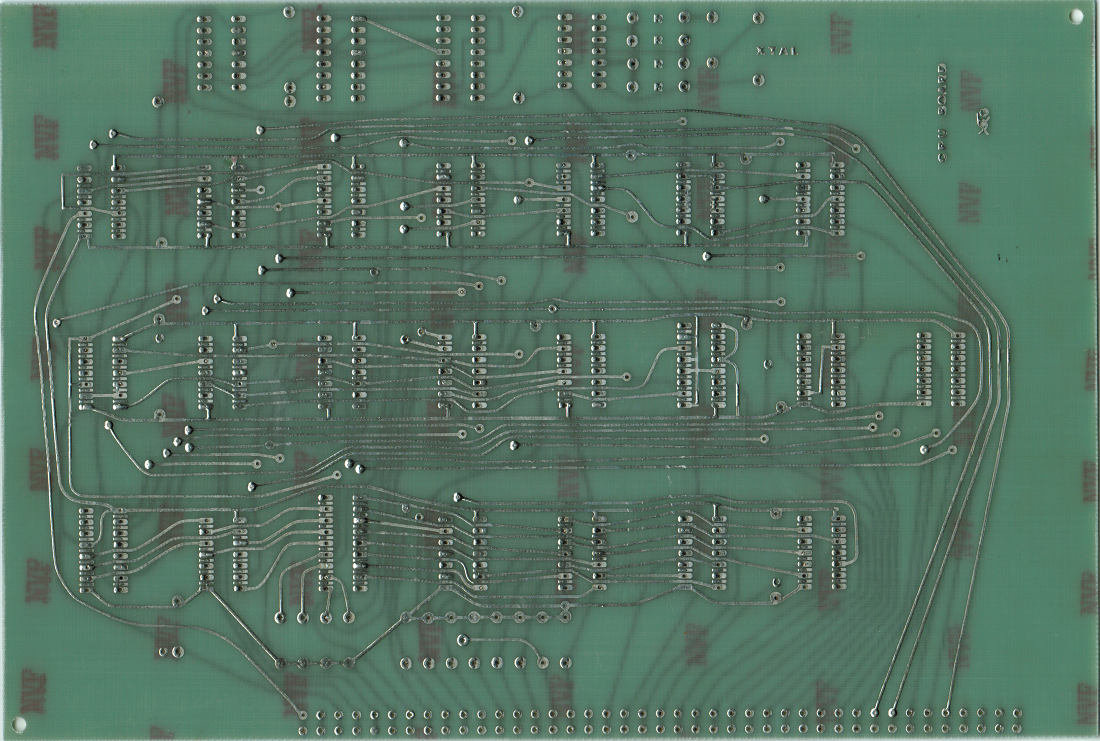
After the molex connectors were installed, I decided to try installing the Timing board to see how it fit:
Okay so it looks good, but unfortunately it turns out I was indeed a victim of scan skewing. One of the molex connectors is skewed just slightly off to the right, so it is not straight in line with the others and requires an uncomfortable twisting of the back end of the Timing board to get it to mate. I ended up removing the Timing board and adjusting the pins as I had them pointing outward somewhat rather than straight down. This helped, and the Timing board now snaps much better into place!
That’s all we’re doing today! Looking good so far!
The timing board is now nearly finished, save for jumper wires:
I’m pretty satisfied, although the real test will be how it cleanly it mates to the motherboard. I recently got my hands on an original Mark-8 construction guide (thank you, Roy!) and found out just how much scanning distorts PCB artwork. It doesn’t just change the scale, it actually skews the artwork. This means in situations where you need parts to align, like the molex connectors that the boards stack onto, you need to check to make sure it all lines up, at least. Being that these were my first ever homemade PCBs, I didn’t think to check that. Ulp.
There are a few caps and a whole whack of jumpers missing; those will be installed later. I’m not liking the new style caps at all — I think those will be revisited. I’ll get into the whole caps affair in another post.
Having done a bunch of jumpers on my ASCII encoder, I know this will be the least fun bit of the whole project. I will do them all on all four boards while I await the last parts. For now, I’m sticking to main components (ICs, caps, diodes, resistors, connectors).
Also, as I mentioned, I’m using sockets for all of it. This is one clear break from the prototype — from the photo it’s clear Don soldered all his ICs in directly. For an experienced electronics engineer this is doable, but for a self-teaching novice using 40+ year old ICs, this would be the definition of insanity. It’s just so much easier from a troubleshooting standpoint to be able to swap ICs. So, that’s how that goes. However, in keeping with the hobbyist/prototype theme, I’m just using what sockets I have lying around that look correct vintage, rather than trying to make every one the same. I think that gives the unit a more earthy feel.
I’m also keeping an eye peeled for solder bridges, and even accidental bridges from the toner transfer/etching process. The construction guide warns you about these, and indeed, they were the major thing that prevented my ASCII encoder from working right off the bat.
Anyway, we’re done here for now.. onto the ‘mainframe’ (motherboard)!
As I mentioned earlier, I had been procrastinating on starting my TVT build for months. I had it in my head that I could not begin until I had everything, and could build the boards sequentially starting from mainboard up to all the others. One reason for this was I wasn’t really sure how some components would fit. Thus, I might want to drill holes larger than I had in the PCBs. This is trickier to do when the boards have parts installed.
In the end though, I realized it could be a while before I found the remaining parts I needed, and if I didn’t get going soon with each passing day I might not ever.
So I decided not to go sequentially, and picked a board to start with. The Timing board seemed like a nice one – fairly straightforward. I had all the parts necessary except the crystal, which I’m working on.
The first bit of business was getting the molex connectors for the device’s bus in place. Initially I couldn’t quite visualize how all this went together. There is a female molex connector that sits on the top, non-copper side of the PCB. Like so:
It is soldered in on the bottom. The connectors are arranged in such a way that pins installed and soldered beside their own pins underneath line up and press into the connector beneath.
My concern primarily was how to ensure the pins were strong enough to sustain the force necessary to slide in. Throughout the course of the build and testing, and later on as the unit aged, I’d probably need to repeatedly assemble and disassemble.
Initially I thought about molex headers. I’d mount them such that the plastic casing around them was on the same side as the female molex connectors. But this wouldn’t work — the molex connector overhangs the hole where the bottom pins come up. Nothing could fit under there. I ended up buying headers with the pins spaced incorrectly on purpose, just so I could pull the pins out one by one and solder them like so to the PCB:
Once you see it in person, it starts making sense. The long individual pins basically slide through their hole and butt up under the lip of the molex connector up top. It doesn’t matter if they make contact with the molex connector’s own pins – they’re all on the same trace anyway. Then it’s just a matter of getting the pins aligned properly and soldered in.
I should mention that one other worry I had about this setup was that these pins would be vulnerable to breakage. There’s really not much holding them to the board.. just the thin slice of copper trace they’re soldered to. But a quick test proved they were more than strong enough to hang on through several plugging/unpluggings. I did have to repeatedly adjust to get them nice and straight and spaced evenly, but eventually I got the first row done:
For several months, not much progress has happened on the TVT. An attention-challenged collector, I’m always being tempted by other things. I ended up making a few more acquisitions in the last few months, including a second SWTPC 6800 system, a Netronics video terminal (and homebrew Z80 computer), a Jupiter Ace.. oh, and did I mention I scored some original Mark-8 boards? 🙂 I also got wind of another possible project – building a replica of the original SOL Terminal prototype. I actually discovered I had the proper keyboard to do it! But I digress.
Part of my problem with getting going on the TVT was knowing where to start. My logical brain said: go with the mainboard. But I didn’t have the transformers, nor some other odds and ends, and I kept delaying. Eventually I realized time was passing quickly, and maybe I could just build what I could and get going, and then fill in the blanks later?
So that’s what I decided to do! I decided I’d not care what order I went, I’d just make sure I was building the TVT every day I could, a bit at a time. Whatever I could do, I would do. That’s the only way to get there. Otherwise, procrastination leads to a dead project.
One detour before I built though, I decided I wasn’t quite satisfied with the colour of my boards. They just don’t look vintage enough in my eyes, up close. The old process of making PCB substrate (the fibreglass/plastic the copper traces are attached to) produced something that was somewhat fluorescent. That process was problematic and is no longer in use. Today’s boards tend to be either brown, or yellow, or a very light yellow green. I chose the latter since that was as close as I could get to the kind of vintage green you see on originals. Even now, I’m still not wild about it. I’ve had some crazy thoughts, like getting a piece of original substrate and having it replated with copper and then I could etch it. But, finding original substrate is almost impossible and the cost to do all that would be exorbitant. How about dyeing?
Yes, apparently you can dye PCBs. It’s simple. You get some Rit fabric dye, a pot your spouse won’t mind you destroying, and throw it in some hot water and boil your PCB until it attains the color you desire.
I decided, looking at my boards, they weren’t green enough. They were more on the yellow side, so, drawing on my experiences as an art student in the ancient past, thought I’d try using blue dye to green it more. Royal Blue, to be exact.
First, a comparison of colour. On the left, my new TVT mainboard. On the right, an original Mark-8 CPU board. You can see the difference right away — the bright fluorescent hue. This is likely impossible to reproduce with dye, but let’s see how close we can get.
The instructions say you mix up the dye separately in a cup or so of hot water, and then add to your hot pot. I guess this is to prevent clumping of the dye powder.
Next you need to build an apparatus to allow the board to be suspended in the pot. I don’t have any photos of my mainboard being dipped, but I do have photos of a Mark-8 reproduction board I was working on simultaneously:
I had the oven on high for about an hour. I didn’t notice any difference on inspection. I then left it simmering, for an hour, then two, then turned it off and left it overnight. I still wasn’t noticing a difference, so I decided to add more dye. Within an hour, there was a striking difference. Here’s two of my repro Mark-8 boards side by side just to give you an idea. One is undyed.
Quite a difference with the dye, huh? And here’s a comparison shot of the dyed Mark-8 board against that same board and an original SWTPC GT-6144 graphics board:
Unfortunately, not the correct color for the Mark-8 boards produced by Techniques, but could be legit as a totally home brew. And close to SWTPC, which provided the original TVT boards in the kit Radio Electronics offered.
I dyed my TVT boards with this stronger batch of dye. I ‘blue’ it!
Oops.
Definitely a little heavy on the blue. I can live with it, but a note for next time: keep the amount of dye relative to water light. My SWTPC boards went into the dye after I had doubled the blue, and so consequently the blue sunk in much more quickly. Further, the manufacturer of the boards I used for my TVT is a different one than my Mark-8. Subtle differences in the substrate result in different colors. That said, some of the boards I put in after the mainboard benefitted from that lesson, and actually came out pretty close to original colour. Check out the Timing board here vs. an original P197 SWTPC power supply board:
I mean, that’s kind of as close as I think you’re going to get with new substrate. Gotta be happy with that.
Lesson learned: more dye = less soaking time, less dye = more.
Okay so on my last post I had tweaked artwork and set up for trying to make a copy of my Mark-8 CPU board. I got my double-sided copper clad in yesterday and am raring to go!
In terms of process, it’s very similar to what I went through with my TVT boards. The difference this time is I have an original for reference and can be a bit more confident that my work is good.
The first thing was to print out the artwork on my favourite Hot Rod Magazine paper. I don’t know why but this stuff transfers really well.
The challenge with doing a double-sided board is getting both sides to align just-so so that your ICs and components will install easily. This is why I went to some lengths to make sure the artwork matched properly in Photoshop. Now I had to align it on the copper clad.
The strategy I settled on was to drill holes in a couple of IC and resistor pads up top and below. I reasoned that these were so small that if they aligned okay, I knew I’d be good. I then made holes in the appropriate places on the artwork. I used a small piece of wire to go through the PCB and transfer paper and bent on one side to secure. I did this in three locations just to be safe. In the first photo you can see the little pin through on the other side.
Basically from there it was just carefully aligning the transfer sheet for side two to those pins, and once the pins were through bending them to hold it in place. Then I took some scotch tape and pressed it down on the corners to hold. I didn’t want the pins staying in and damaging the iron or ripping the paper, obviously as I ironed.
Ironing went fairly smoothly, however I did note that the resulting heat caused the opposite side I was ironing to actually smudge the toner in a couple of places. Hrmm. Not sure how to get around that. Perhaps having the ironing happening on something cool? The counter top does get pretty hot when I’m doing this.
When I dipped the boards into the cooling bath and removed the paper, I discovered, as usual, the iron had missed in a few places. Almost always does. So I did touching up with nail polish to fill gaps.
Anyway, once that was done, I used my original board (very carefully) as a guide to trace cutting lines so I could cut the board to be the exact same size. Voila, side by side:
Next was etching. I’m still wussing out from using heavier stuff like my ferric chloride. I think I might be getting over that. One problem with using the friendlier vinegar/peroxide/salt etchant is that it takes a ton of it to etch boards this big. I used 6 500ml bottles of peroxide and an equivalent amount of household cleaning vinegar. It took something like 2 hours to etch off the acres of copper on this board that needed to go. And unfortunately that’s too long for the nail polish ‘patches’ to hang on. The nail polish eventually lets go and that copper becomes exposed. I had to apply it again to try and save those traces, but a few were eaten right though.
Overall the result after etching isn’t too bad. Side 2 came out really nice and clean. I think I have to do more work on Side 1’s artwork to make the traces a bit darker and a tiny bit thicker.
Lastly I took some acetone and wiped away the toner. Then I drilled out some of the pads to test how both sides aligned. I’m delighted to say the alignment is just a hair off in a few places. But otherwise, it’s darn near perfect, especially considering the bozo (me) trying to align them.
So there you have it. I’m going to use this board as an experiment piece. I want to see if dying it with some blue or green Rit dye gets me a bit closer to the color of the original (right). Then I’ll learn about tinning, and just see how close I can dial it in.
To recap: I need to figure out how to better transfer toner. I’ve stuck with ironing because it has served me well. My laminator did not do a good job and these fancy transfer papers seem to be even less reliable than my magazine paper. I also need to maybe adopt a better etching process. But for a first try, I’m pretty happy. This gives me confidence that the end goal is attainable.
Christmas is done (yay!) and now I have a bit of free time before we go back to work for vintage computer projects. And what better way to close out the old year and ring in a new one by attempting to clone Jon Titus’ Mark-8 boards?
In earlier posts I detailed my adventures in recreating the board set for Don Lancaster’s TV Typewriter. That project is still ongoing, but by far the most fun I had was taking scans of the original artwork and then transferring that onto copper, and I’ve been looking for excuses to make new PCBs for something else.
Recently I acquired some original, untouched Mark-8 boards on Ebay. That remains the pinnacle of my collecting career, given how rare these are. However I bought them without really thinking through what it meant. Boards alone do not a computer make, and to take a soldering iron to these means risking damage, both literal and in terms of value. There are only around 20 or so Mark-8s known to exist, and of those, only mine and one other set are known to be unbuilt.
I’m not totally against building them though. I solicited opinions all over the place and many were of the mindset that a computer is pointless if it doesn’t do anything.
It’s a tough one. But in the interim, there’s no crime against history in recreating some new boards. At the very least, I can use them as practice runs for potentially building these ones one day. Better to learn on something that isn’t virtually irreplaceable first. I’m therefore setting a goal of recreating new boards that look as close to the originals as possible. I’ve even read up on how to dye my new PCB stock to more closely match the color of the original, and even how to create a stamp to mark the boards with the similar marks the PCB fab house would have used.
To be clear, cloning the Mark-8 boards has been possible all the way back to day one. The original construction guide provided the artwork to make your own. In fact, Steve Gabaly (aka Obtronix) took copies of said artwork and produced a kit, which some unethical types occasionally tried to pass off as original on Ebay. I’m told these kits had some issues, owing to the quality of the copied artwork they were based on.
I had actually planned to go the same route myself using a PDF of the construction kit Bryan the ‘Byte Collector’ was kind enough to scan and put on his site. That had been my original ‘get a Mark-8’ plan going back years. I “knew” the odds of affording, let alone seeing a Mark-8 for sale anywhere were slim to none.
I was warned though not to trust the construction guide copies found online. Copying and scanning does funny things to artwork. I ran into this on my TVT build: the artwork had to be scaled up slightly to fit components properly. Lacking an original TVT to compare to, I’m still not sure I’m 100% in the zone, but checking against ICs and components, they look right.
An additional challenge: Mark-8 boards, unlike the TVT, are double-sided. I’ve never made double-sided boards before. I’m lucky the originals weren’t (for cost reasons) through plate – I’d never be able to do that myself, so at least mine can still be in keeping with the originals that way. But I know lining up two distinct pieces of artwork and making it come together just so will be a huge challenge for someone of my limited skills.
However, I do have the advantage of having the original boards to compare against. Further, a Mark-8 clone would be the perfect companion to my TVT clone – both were signature Radio Electronics magazine projects, and in fact the Mark-8 information mentioned the TVT as a possible interface device.
Now, originally I was just going to import the scanned artwork into Photoshop and then keep tweaking the size and printing it until the IC pads fit the ICs, which I have. But since I have the originals, I have an advantage others didn’t. So what I’ll do is actually scan the originals on my scanner. That’ll give me something visual onscreen to compare to.
The first thing I did was put it (gently) on my scanner. I didn’t need anything high-res here, just good enough to clearly see the traces. The result (of the first side):
A direct scan of my original Mark-8 CPU board.
Pretty elegant, huh?
After converting the artwork in the PDF to JPG, I then imported the first side of the CPU board artwork into Photoshop. Next, I opened up the scan I made of the original in a separate window. I realized I had to do a bit of scaling to get the artwork into roughly the same size as the original. So I went back to the artwork, rescaled it, and then used the marquee tool to highlight and copy all of it. Now I brought it over into the other window and pasted it as a second layer. This of course completely obscures the original board below, however by changing the opacity of the new layer (called Layer 2) over on the right side of the screen, I can make it so that I can see through the artwork I’ve pasted to the original below. This will help me align the two and do any changes necessary to make them as close as possible.
Okay so obviously I needed to further reduce the size of the artwork, which I did. However, reducing wasn’t enough. Looking at the two interspersed with each other it became really apparent just how skewed the scanned artwork was. It wasn’t, like the TVT, just a matter of being the wrong size. It was actually distorted in a sort of trapezoidal shape. Thank goodness I had the originals to rely on. If I’d tried to make a go of it with these, I’dve been hopelessly lost!
Anyway, since I have the original to use as a guide, I’d just have to make use of the appropriately named Distortion tool, and Skew tool, to fix the messed up artwork. After half an hour of carpal tunnel-inducing fine mousework, I had them more or less aligned. The screenshot below shows me about 90% of the way there:
After getting it the rest of the way, returned the opacity to 100%, did the marquee tool and copied the now-corrected artwork back over to the original window. After clearing that window and pasting it there, I then flipped it horizontally (since I intend to use the toner transfer method again this is necessary to prevent it from producing a mirror image when applied to the copper clad board), whitened up the background and saved it. Then I printed it off and using a bright light behind compared it to the original board. It aligned almost perfectly!
Having completed that side, I turned my attention to the other side of the CPU board. I followed the same process, scanning the backside of the original, importing the artwork and so on. The back side was even worse than the front. It was way off, and I really had to work that distortion tool to get it correct against the original.
After completing and saving it, I decided to check not only how it compared to the original but how it lined up with the first side artwork I had fixed. To my surprise, it didn’t quite line up right. In fact, some of the bus holes were as much as several mm off!
Hmmm.. how to fix that. Aha! I’ll use the two sides of the corrected artwork and align them against each other. I figured the easiest way to achieve this was to invert one side (making the black and white colors reverse), and then copy the other side over it, and set opacity down to 50% on the copied layer.
Then it was just a matter of making the black traces of the copied layer line up with the white ‘spaces’ of the inverted layer.
It took a bit more finagling, some rotation and so forth before I had it pretty much dead on. Once that was done, I again brought the opacity of my Side 1 layer back to 100% and then copied over to a new, clean window. I reversed the inversion on Side 2 and saved both.
Now I have nice , fairly correct artwork for the first board:
Yes, I did make one tiny alteration. The construction article artwork doesn’t have the manufacturer’s (Techniques) mark right beside where it says ‘CPU BOARD’. I actually copied that from my originals, converted to black and white and touched it up and then pasted it to my artwork.
The print copies of the artwork line up nicely when put together:
And they look pretty good dimensionally next to the original board:
The artwork is nice and dark and should transfer pretty nicely. I can’t wait for my double-sided PCB stock to arrive so I can try it out!
If you’re a collector like me who lives on a budget, there are realities you have to accept. You’re never going to own an Apple-1, for example. There’s only about 50 of them left out there, many in museum hands. And then there’s the matter of value – being so rare, they’re worth more than houses.
One way to compensate for this reality is to recreate what you cannot buy. That was the approach I took with my TV Typewriter project. And in fact, I have an Apple I replica board on my desk, waiting to be assembled.
And that was the approach I had planned to take with Dr. Jon Titus’ 1974 Mark-8, the third microprocessor based computer (based on Intel’s 8008) ever offered to the public. The plans with PCB artwork are out there, and so are the vintage components. All it takes is the time, money and will to make one.
No, the Mark-8 wasn’t first. That honour belonged to the French Micral. Second place belonged to the American-made SCELBI. But there is something really special about Radio Electronics’ early ventures into computing. The magazine for ‘Men With Ideas in Electronics’ pioneered things we take for granted, like video terminals and keyboards. The Mark-8 was a kind of coup de grace, at least in the months before Popular Electronics responded with the Altair.
The Mark-8 was a tough project. Apart from offering a few board sets produced by a New Jersey company called Techniques, everything else was up to the hobbyist, including finding the ICs and parts and assembly. You had to find all that, follow schematics and bridge several pieces of missing information and errors. According to Byte Collector Bryan Blackburn, Jon Titus estimated 7500 plans were sold, and only about 400 board sets. To date, only just over a dozen Mark-8s are known to exist. So you’d think the odds of an average collector happening upon some in the wild, and being able to buy them at a reasonable price would be nil, right?
But you’d be wrong:
When I first saw that auction come up, I couldn’t believe my eyes. I don’t have any followed searches for ‘Mark-8 boards’ (why would I search for something impossible to find?). Rather my followed searches simply look for ‘boards’ listed in EBay’s Vintage Computing section. When I saw these I just about fell out of my chair. I had read, with envy, how Bryan had found his Mark-8 boards some years ago much the same way. I thought the odds of that ever happening again to be impossible. But there they were.
Anyway, I threw in a bid. The last time a Mark-8 sold, it went for over $5000USD, and that was 9 years ago. These appeared to be untouched, almost pristine condition original boards. I was sure a heavyweight collector would easily drop thousands on them. But I figured it’d be fun to pretend to own them for a while. I set my initial bid at $1000USD. And it held out the full 9 days, all the way until just the last minute, when somebody bid up to $1300. Believing these were never going to be mine anyway, as a lark I upped my bid to $1575. Then I watched the last seconds tick away, waiting for that last snipe to take ‘my’ boards from me. But it didn’t happen. The price settled at $1517. I was now a member of an extremely exclusive club: Mark-8 owner. Okay, they’re just the boards, but still. Untouched? How rare is that? I felt almost paranoid — had I been had? Just a few a years earlier someone on ebay had tried to pass off an Obtronix reproduction kit as original. Were these really good fakes that real collectors had spotted a mile away?
I did a lot of asking around, but the consensus was, they were the real deal! The original Techniques bags nailed it, along with the unique fab house markings on the PCB substrate. Wow!
Ladies and gentlemen, I present one of the few Mark-8s, in unbuilt board form, not in American hands:
It’s so weird to hold something in your hands that ordinarily you’d only be able to see encased in a glass box at a museum. This is such an important piece of computing history and it’s a real privilege to have it, to be able to look at it any time I want!
The only negative is I now find myself squarely in the situation I would have been in had I won some original TV Typewriter boards that appeared on ebay. I am in a very unique position that no one else is presently: I can build a real Mark-8. It’ll never be ‘original vintage’ of course, but I could assemble a machine that was otherwise indistinguishable from an original – using available vintage components!
The advice I’ve gotten on the matter is all over the map. Preservationists argue the untouched boards like these are so rare they need to be kept as is for posterity. But others take a more pragmatic view: that computers were designed to do something, and that leaving the boards unbuilt robs them of the chance to do what they were designed to do.
What do you think? Nothing is going to happen any time soon — I simply don’t have the skill to build a Mark-8, yet. But comments are most welcome!